
Moore’s Law Is Dying. TSMC and Intel Just Chose Opposite Ways to Survive.
One Is Building a Bigger City. The Other Is Inventing a Better Brick. Only One Strategy Will Win.

For fifty years, the semiconductor industry ran on one rule: make the transistor smaller, and everything gets faster. You did not need a strategy. Physics did the work. Every new generation of chip delivered 30 to 50% more transistors on the same surface area, and the entire digital economy rode that escalator upward. A single, consistent dynamic fuels everything from your phone and laptop to artificial intelligence.
Reduce the size of the transistor.
Make the gains.
Repeat.
That rule is dying. And how the two companies that matter most in semiconductor manufacturing respond to its death will reshape the chip industry for the next decade.
The Wall That Physics Built
When a transistor is just a few nanometers across, you are working at the scale of a few dozen atoms. At that scale, electrons stop behaving the way classical engineering expects them to. They start tunneling through barriers they should not be able to cross, a phenomenon called quantum tunneling. Once that happens, shrinking the transistor further yields almost no performance gains. The engine that drove fifty years of exponential improvement in computing simply stalls.
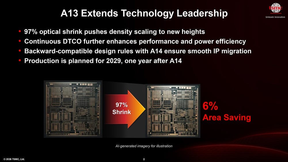
TSMC, the Taiwanese foundry that manufactures virtually all the world’s most advanced chips, unveiled its technology roadmap through 2029 at its North America Technology Symposium on April 22, 2026. The new nodes announced — A14, A13, and A12 — sound like enormous progress. 14 angstroms. 12 angstroms. An angstrom is one-tenth of a nanometer. We are talking about features measured in handfuls of atoms.
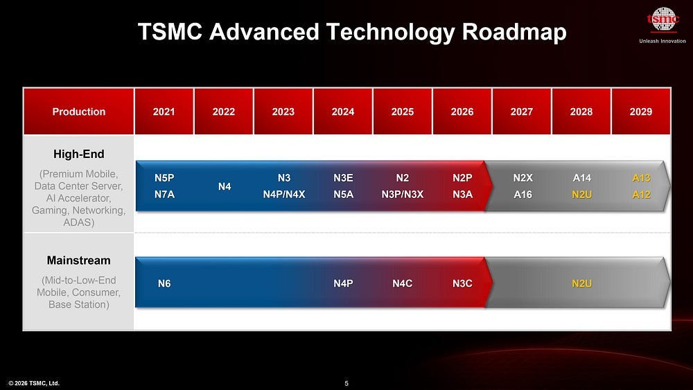
But the real gain between these generations is approximately 6% in transistor density.
Six percent.
The demand for AI compute is growing exponentially at this moment. That gap between what physics can deliver and what artificial intelligence requires is the central tension in the entire semiconductor industry right now.
The Quick Fix That Bought Time
The industry found a temporary solution. They changed the shape of the transistor itself.
For more than a decade, advanced chips used an architecture called FinFET: a three-dimensional transistor structure where the gate (the part controlling current flow) wraps around the channel on three sides. It is the architecture that allowed your smartphone to become as powerful as a desktop computer from ten years ago. But at today’s scale, three-sided control is no longer enough.
The replacement is called Gate-All-Around, or GAA. The principle is elegant: instead of a single fin, you stack multiple nanosheets on top of each other and wrap the gate completely around each one. Current control becomes total. Current flows when it should, stops when it should, and crucially, does not leak between states. TSMC deployed GAA for the first time with its N2 node, which entered mass production in late 2025. Intel developed its own version called RibbonFET, the same physical principle under a different name, because in semiconductors, nobody likes using the neighbor’s vocabulary.
Gate-All-Around is real progress. But it does not restore the old gains. It maintains the trajectory under life support. It was the quick fix. And this is where the two giants diverge.
TSMC: Build a Bigger City
TSMC looked at the problem and made a cold decision. If shrinking transistors now delivers only 6% improvement per generation, they would stop betting primarily on the transistor. They would bet on the system.
Instead of grinding toward ever-smaller features on a single chip, TSMC takes multiple chips — compute dies, memory, interconnect layers — and assembles them into what amounts to a mega-package. The reason they have no choice is a physical constraint that few people outside the industry know about. Inside an EUV lithography machine, the light can only expose a small rectangle of silicon per pass: approximately 26 by 33 millimeters. This is called the reticle limit, and it is a hard physical ceiling. You cannot make a chip larger than that in a single exposure.
So TSMC stopped trying. Instead of building one giant chip, they assemble dozens of chips into a package that exceeds the reticle limit entirely. At their April 2026 symposium, they presented packages combining up to 10 compute dies with 20 memory stacks, planned for 2028, using 14-reticle CoWoS integration. The frontier of performance has moved. It is no longer inside the transistor. It is in how you connect the pieces.
But this strategy creates a new bottleneck. When you place that many chips next to each other, the constraint is no longer computation — it is communication between chips. The GPU needs to access memory. Memory needs logic. Data must flow between all components at an enormous bandwidth without the system literally melting under the thermal load. This is exactly where TSMC’s advanced packaging technology, CoWoS (Chip on Wafer on Substrate), becomes critical infrastructure.
Nvidia understood this before anyone else. The company has reserved more than 60% of TSMC’s global advanced packaging capacity for 2026, approximately 595,000 wafers for the year, with 510,000 of those allocated to CoWoS alone. TSMC produced roughly 35,000 CoWoS wafers per month at the end of 2024. Their target for the end of 2026 is 130,000 per month. Quadrupling monthly capacity on a process this complex in 24 months is unprecedented. And even that is not enough. TSMC has been forced to subcontract packaging work to ASE and Amkor, something that would have been unthinkable three years ago. TSMC is gradually moving 10 to 20 percent of its anticipated $56 billion in capital expenditures for 2026 into packaging equipment.
And then TSMC made a decision that shocked the industry. They said no to High-NA EUV.
The $400 Million Machine TSMC Does Not Want
High-NA EUV is the latest generation of extreme ultraviolet lithography machines built by ASML in the Netherlands. Each machine costs approximately $400 million. It pushes optical resolution further, enabling finer patterning. On paper, it is the future of chip fabrication.
TSMC’s published roadmap through 2029 does not use High-NA EUV for any node.
Not A16.
Not A14.
Not A13.
Not A12.
None of them.
AI Is Eating the World’s Memory. Apple Is the Only Company That Doesn’t Care.

There’s a component inside every device you own that you’ve probably never thought about. It’s called RAM: random access memory. Without it, your processor is a genius sitting in an empty room with no desk, no paper, and no way to work. RAM is the surface where your computer spreads out everything it’s doing at once: every open tab, every running applic…
The reasoning is both simple and brutal. High-NA pushes resolution further but reduces throughout. Each wafer costs more to produce. Yield risk increases. And in semiconductor manufacturing, the difference between a laboratory triumph and an industry is the ability to do the same thing millions of times at an industrial scale. TSMC makes more than a chip per second. That is the discipline. Instead of adopting new lithography hardware, TSMC is pushing its existing EUV machines further using a technique called multipatterning:
Exposing each layer multiple times at slightly different angles to achieve finer features than a single pass could produce. It is slower. It is more complex. But it is controlled.
TSMC chose reliability over spectacle.
Intel: Invent a Better Brick
On the other side of the Pacific, Intel is doing the exact opposite. They are going all in.
Intel has already implemented High-NA EUV machines into its development process for the 18A node and future advancements. For transistors, they are deploying RibbonFET. For power delivery, they developed PowerVia, a technique that delivers electricity through the back of the wafer rather than the front. This is the first time in 60 years of semiconductor manufacturing that signal routing and power delivery have been separated onto opposite sides of the chip. For die-to-die communication, they are moving to co-packaged optics: replacing copper interconnects with light to move data between chips.
Each of these innovations is impressive. The problem is that Intel is stacking all of them simultaneously in the same process on the same chip. There is an unwritten rule in semiconductor manufacturing that everyone knows: do not change too many variables at once. When something breaks in a process that is moving on five fronts simultaneously, finding the root cause becomes a nightmare.
Intel’s path is nonlinear.
Should things go as planned, they’ll establish a substantial lead in the industry.
If a single link in the chain fails, recovery will be long and painful.
Until recently, almost nobody believed Intel could pull it off. Then something changed.
The Signals Nobody Expected
The first Panther Lake computers, built on Intel’s 18A node, have been on sale since early 2026, with over 200 machine designs shipping. The 18A process is the first 2-nanometer-class chip entirely designed and manufactured in the United States. Production yields are reportedly running ahead of internal targets, hitting end-of-year benchmarks approximately two quarters early.
But yields are not the strongest signal. The order book is.
On May 8, 2026, the Wall Street Journal reported that Apple and Intel had reached a preliminary agreement for Intel to manufacture certain Apple processors on its 18A node. The same Apple whose outgoing CEO, Tim Cook, had previously told Morris Chang, TSMC’s founder, that Intel could not make chips, that it was a bad foundry, and that Apple would never go back. Intel stock hit an intraday high of $130.57 that day, clearing its dot-com era peak from the year 2000 by roughly 72%. The stock is up approximately 521% year-over-year.
Taiwanese analysts are clear: Apple is not abandoning TSMC for its flagship chips. The A-series in iPhones and the M-series in Macs will stay with TSMC. The motivation is strategic. Create negotiating leverage. Reduce geopolitical exposure to Taiwan. Prepare a contingency if the capacity of advanced nodes continues to shrink. But even a limited deal on entry-level chips changes the entire industry’s perception of Intel as a foundry.
Then, on May 10, Jensen Huang received an honorary doctorate at Carnegie Mellon University. It was Lip-Bu Tan, Intel’s CEO, who presented it. During the ceremony, Tan publicly declared that the two companies would work together on “exciting new products.” NVIDIA invested $5 billion in Intel earlier this year. Industry sources indicate that upcoming Nvidia GPUs on the Feynman architecture could use Intel’s packaging technology for assembly and the 18A or 14A nodes for certain components. When the company that monopolizes 60% of TSMC’s advanced packaging capacity starts looking for alternatives, the structural logic is unmistakable.
And then there is TeraFab. In April 2026, Intel officially joined the project led by Elon Musk. The concept: a mega-factory in Austin, Texas, capable of producing logic, memory, and advanced packaging under one roof. Tesla manages the pilot research line.
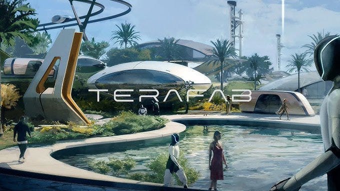
SpaceX handles mass production. Intel provides the lithography technology, likely its 14A node under license. C.C. Wei, TSMC’s CEO, responded with characteristic restraint: there are no shortcuts in the foundry business. Building a fab takes two to three years minimum, and scaling production takes another two to three on top of that.
Musk Just Announced a $25B Chip Factory That Nvidia’s CEO Says Is “Impossible.”

March 21st, 9 PM, Austin, Texas. Light beams pierce the sky above a decades-abandoned power plant. The Texas governor is in the room. Millions watch live on X. Elon Musk walks onstage and announces a $25 billion semiconductor factory capable of producing, by itself, 50 times more computing power than the entire global AI chip indust…
He is right. He is also the same person who people were when they said SpaceX could never land a rocket on a barge in the middle of the ocean.
A Bigger City or a Better Brick
The contrast between these two strategies is striking. TSMC has decided the transistor is no longer the primary lever and is rebuilding the entire system around that reality: packaging, integration, scale. Intel believes the transistor still has secrets to reveal and is pushing physics to its absolute limits, risking everything on a single hand.
I think both are right, but in different ways. The problem is that in this industry, one model always ends up dominating. The metric that will decide the winner is not transistor size or patent count. It is a purely economic law:
Cost per unit of compute at scale. And behind that metric, driving all of it, is artificial intelligence.
What is genuinely fascinating is that for the first time in a decade, this question does not have an obvious answer. Three months ago, if you asked anyone in the industry who would win, the answer would have been TSMC without a second thought. Today, with Apple, Nvidia, and TeraFab appearing in Intel’s order book, real uncertainty has returned to a contest that had seemed settled.
What is certain is that this war between two giants will determine who has access to computing, at what price, and in which country it is manufactured. And that question, in 2026, is no longer an engineering curiosity. It is geopolitics, economics, and the infrastructure of artificial intelligence, all converging on the same strip of silicon.
Thanks for reading. Your opinions are welcome in the comments to explore this topic.