

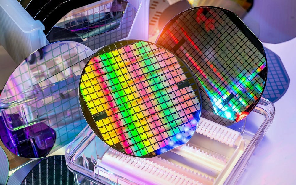
Silicon has ruled the chip industry for 60 years. Every calculation happening on this planet right now, from your smartphone to the processors powering AI, runs on this one material. And for the first time, the industry has officially named what comes next.
A few weeks ago, IMEC unveiled its updated technology roadmap for the coming decade. IMEC is the organization that sets the direction for the entire semiconductor industry. They work with the world’s largest chip makers, such as Intel, TSMC, and ASML. On that roadmap, something remarkable appears. Around 2041, silicon disappears from the transistor itself. The material taking its place is three atoms thick.
The Wall That Physics Built
For decades, the industry progressed by doing one thing: making transistors smaller. Smaller meant faster and cheaper. That formula worked for 60 years until it hit a wall.
Not an economic wall.
A physical one, imposed by the laws of physics themselves.
When transistors approach atomic dimensions, quantum effects start showing up. The most dangerous is quantum tunneling, the phenomenon where electrons stop behaving like particles and start acting like waves. Waves pass through barriers. The transistors are leaking. Current flows where it’s never supposed to, and when your chip contains billions of these tiny switches, that’s a problem you can’t engineer around using conventional materials.
Every time the industry thought it had reached the end, engineers found a workaround. Transistors went from flat to three-dimensional fin structures (FinFETs). Then the gate wrapped entirely around the channel in what’s called gate-all-around architecture. Intel integrated this into its 18A node with nanosheets, horizontal bars so small that current passes through them, combined with backside power delivery that feeds electricity from underneath the chip instead of cluttering the already saturated top layer. Two of modern chip-making’s most complex problems, solved in a single device.
The next step is called CFET, where you stack two transistors on top of each other in the space one used to occupy. According to IMEC’s roadmap, commercial introduction is expected around 2033 at the angstrom-scale node. Each generation has bought silicon another reprieve, but CFET will probably be the last.
After that, the channel material itself changes.
A Lubricant That Became a Semiconductor
Silicon gives way to a family of materials called 2D semiconductors. The candidate leading the race is molybdenum disulfide, MoS₂. The name doesn’t exactly roll off the tongue.
Its structure is simple: a layer of molybdenum atoms sandwiched between two layers of sulfur atoms.
Three atomic layers in total.
Half a nanometer thick.
The abundance of both molybdenum and sulfur has a considerable impact on the supply equation.
The genuinely amusing part is that we’ve known about this material for centuries. In its natural form, it’s called molybdenite. For most of history, people confused it with graphite or lead ore. The word molybdenum comes from the Greek “molybdos,” meaning lead. It was used as an industrial lubricant, grease for heavy machinery. If you’d told a chip engineer in 2005 that the grease in their factory would one day sit at the heart of the world’s most advanced processors, they would have laughed you out of the room.
What truly makes MoS₂ so promising is that for decades, the industry has been working on thinning silicon. MoS₂ starts thin. That’s its entire advantage. The thinner the transistor channel, the more precisely the gate controls the flow of electrons. Better control means a lower operating voltage. And in semiconductor engineering, lowering the voltage is everything. Energy consumption scales with the square of the voltage. Cut the voltage in half, and you cut consumption by a factor of four.
In theory.
Published research shows MoS₂ transistors consuming up to 1,000 times less energy than comparable silicon devices.
