
The Death of Moore’s Law Just Kicked Off a Three-Front War — and Nobody Told You About It
TSMC achieved the impossible. Then, Huawei, IBM, and OpenAI each announced they no longer need it. Something fundamental broke in the chip industry last week, and it changes everything from your next

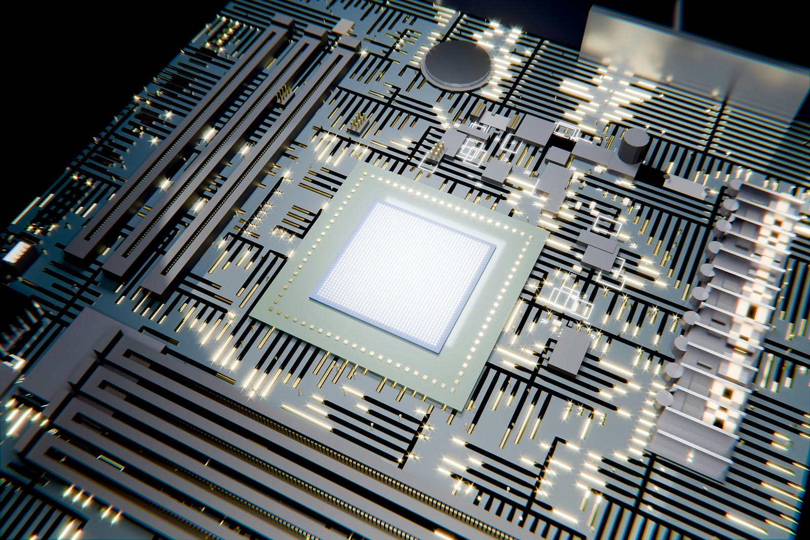
Two nanometers.
That’s about 20 atoms wide. That is what TSMC began producing at volume starting at the end of 2025, ramping hard through 2026. Apple, Nvidia, AMD, Google — they’re all queuing for it. The entire production capacity is booked through the end of the year.
I’ve been following chip technology for a while now, and when I first read the 2nm spec sheet, my reaction wasn’t awe. It was vertigo. We built this. It is 20 atoms wide and switches billions of times per second. Six decades of human ingenuity compressed into a sliver of silicon you’d need a microscope to see.
And then I read what engineers were actually saying behind the headlines. And the vertigo turned into something closer to dread.
The Rule That Ran the World for 50 Years Is Dying
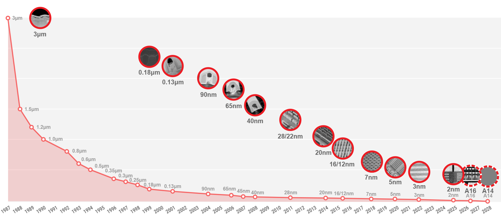
For half a century, the logic was almost offensively simple. Shrink the transistor, get twice the performance. No strategy needed. Physics handled it. The rule is called Moore’s Law — the empirical observation that transistor counts would roughly double every two years — and it’s what took computers from filling an entire room to fitting in your pocket.
But we are in mid-2026. And three major announcements in the space of about a week — from Huawei, IBM, and OpenAI — are all saying the same thing, from three different directions: the era of shrinking transistors as the primary lever of progress is closing.
The strange part is that none of them sounds alarmed. They sound like engineers who’ve already figured out what comes next.
Moore’s Law Is Dying. TSMC and Intel Just Chose Opposite Ways to Survive.

For fifty years, the semiconductor industry ran on one rule: make the transistor smaller, and everything gets faster. You did not need a strategy. Physics did the work. Every new generation of chip delivered 30 to 50% more transistors on the same surface area, and the entire digital economy rode that escalator upward. A single, consistent dy…
The Energy Problem Nobody Talks About at Product Launches
Before getting to the three announcements, you need to understand the actual problem, because it’s not the one being discussed.
More than 80% of the energy consumed by a modern chip doesn’t go toward computation. It goes toward moving information from one point to another inside the chip itself.
Think of a chip as a city. Transistors are the buildings — that’s where the work gets done. The microscopic metal wires connecting them are roads. A modern chip has more than 20 layers of those roads stacked on top of each other. Every signal traveling through those wires encounters two forces working against it: the resistance of the metal itself, which slows it down, and what engineers call parasitic capacitance — essentially a tiny invisible battery along the wire that has to charge and discharge with every piece of information passing through.
The longer the journey, the more both effects compound. Engineers call this the RC delay, and it’s the actual limiting factor in modern chips, far more than transistor size. That’s why processor clock speeds have stagnated for years. Not because the transistors are too big, but because the paths between them are too long.
Once you understand this, the solution that Huawei, IBM, and OpenAI are each converging on looks less like a breakthrough and more like the only logical answer: stop building wider, start building upward.
Huawei’s Seven-Year Secret
About six weeks ago in Shanghai, at the International Circuit and Systems Symposium 2026, He Tingbo stepped back onto a public stage for the first time in years. It’s noteworthy that the leader of Huawei’s chip arm has been largely out of the public eye just as US sanctions have become more stringent. This period saw Huawei cut off from ASML’s EUV machines, the incredibly expensive Dutch-engineered devices essential for TSMC to produce the planet’s smallest transistors.
Without those machines, you can’t go below 7nm with conventional methods. So Huawei’s foundry partner SMIC improvised: they started printing the same pattern in three, four, sometimes five successive passes, where TSMC does it in one.
Clever.
But each additional pass adds defects and complexity. At some point, you hit the ceiling.
That ceiling forced the right question. Is shrinking the transistor actually the right lever?
Huawei’s answer — presented by He Tingbo in Shanghai — is a resounding no. And their alternative has a name: Logic Folding.
The concept is genuinely radical. You take a circuit that normally spreads flat across silicon and fold it in half, like a sheet of paper. Stack the logic layers on top of each other. Suddenly, components that were separated by millimeters of horizontal distance are separated by microns of vertical distance. The signal path collapses. The RC delay collapses with it.
Alongside Logic Folding, Huawei introduced what they’re calling the Tau (τ) Law: a new framework for measuring chip progress not by transistor width, but by signal propagation time across the system. Progress measured in time, not in space.
The claimed numbers are striking: up to 55% higher transistor density, 41% better energy efficiency — without a single EUV machine in the manufacturing chain. Their upcoming Kirin 2026 processor, the first commercial chip to use this architecture and expected this autumn, is reportedly targeting 238 million transistors per square millimeter — comparable to TSMC’s first-generation 3nm node.
There’s a legitimate engineering challenge embedded in this claim. Communication at the necessary speeds between two stacked logic layers relies on millions of copper micro-connections, termed bonding interconnects. The tighter those connections, the faster the layers can talk. Huawei says they’re targeting a bonding pitch of 1.5 microns — compared to roughly 9 microns at the current industry best. That’s six times tighter than anything that exists today. Getting there is not a given. And stacking active logic, which generates enormous heat, inside a smartphone form factor — not a server you can drench in liquid cooling — is the other wall they need to break through.
But here’s what I keep coming back to: the history of technology tells us that constraints produce innovation more reliably than comfort does. When the US cut GPS signals to Europe during the Kosovo War in 1999, Europe built Galileo. When the oil embargo hit Japan in 1973, Japan became the world leader in fuel efficiency. Huawei’s own CEO said it publicly: if America hadn’t forced this, they wouldn’t have done it. Instead of stopping Huawei, the sanctions might have prompted them to develop the next phase of chip technology.
The Week IBM and OpenAI Announced the Same Significant Change, One Day Apart
On June 24, OpenAI and Broadcom unveiled Jalapeño — OpenAI’s first custom-built inference processor. On June 25, IBM announced the world’s first sub-1-nanometer chip.
Two announcements.
Two continents.
One conclusion.
Start with IBM, because the number alone deserves a moment.
0.7 nanometers.
Seven angstroms.
About seven atoms wide.
IBM’s prototype chip, unveiled at VLSI 2026, packs nearly 100 billion transistors onto a piece of silicon the size of a fingernail — roughly double the density of IBM’s own 2nm chip from 2021. The architecture is called Nanostack: instead of shrinking transistors sideways, you stack them vertically in two layers, fabricating each layer sequentially on the same wafer, one directly on top of the other.
According to MIT Technology Review’s reporting, this leads to alignment precision that bonding techniques cannot match.
IBM also cracked open a problem the industry had quietly given up on. SRAM — the ultra-fast on-chip memory that lives inside a processor and serves as the buffer for the most critical calculations — had essentially stopped shrinking since TSMC’s 3nm node. It was consuming a growing share of chip surface area with no solution in sight. IBM’s Nanostack delivers 40% more SRAM density in one move.
For AI workloads that are desperately memory-hungry, that’s not a footnote. It’s a structural unlock.
The honest caveat: this is a laboratory demonstration, not a product. IBM doesn’t manufacture logic chips at commercial volume. It licenses its architectures to partners. The same 2nm chip IBM announced in 2021 is only now approaching wide deployment five years later. Nanostack production is probably five years out. But in this industry, lab demonstrations are the map. And this map shows a clear road below 1 nanometer.
Now, OpenAI’s Jalapeño is a different story. IBM is asking what transistors can look like in a decade. OpenAI is asking what chips should be built right now, and who should build them faster.
The answer to the second question was: AI. Jalapeño went from initial design to manufacturing tape-out in nine months, with OpenAI’s own models accelerating significant portions of the design and optimization process. A design cycle of this complexity would typically take two to three years. They compressed it by a factor of three by using the intelligence built into the models to help design the hardware that those models will run on.
The loop is worth sitting with for a second. AI designs the chip. The chip runs the AI faster. That AI designs the next chip even faster.
Early performance testing shows Jalapeño delivering roughly 50% lower cost per inference than current Nvidia GPUs, with first deployments planned before the end of 2026. Bloomberg reported that Broadcom CEO Hock Tan confirmed the 50% cost reduction figure. This is not an architecture story about what chips might look like in 2031. It’s an economic story about what running AI will cost in six months.
And just like Huawei and IBM, the core principle is identical. OpenAI isn’t competing on transistor size. It’s competing on efficiency, on the compression of time, on the intelligence of the design process itself.
AI Stopped Imitating This Week. It Started Understanding.

For years, the working assumption about AI was simple: it imitates. Feed it enough text, enough images, enough video, and it learns to produce something plausible enough to pass as real. That assumption held up remarkably well, right until the past few weeks, when several teams across several domains released systems that …
What All Three Are Actually Saying
AMD has been stacking memory on processors for three years with its 3D V-Cache. Intel is routing power delivery through the back of the wafer on its latest designs. TSMC is preparing its own version of the same idea.
The era where progress was measured in nanometers of width is closing. What replaces it will be measured in signal travel time, the layer count, design intelligence, and system integration.
This is where things get interesting for anyone paying attention to AI specifically. The cost of running a large language model today is determined almost entirely by GPU compute, and GPU compute is determined almost entirely by the efficiency of the chips running it. If Jalapeño delivers on its 50% cost reduction, and if IBM’s Nanostack architecture makes it to production in five years, and if Huawei’s Logic Folding proves thermal management is solvable, the cost of intelligence collapses.
Fast.
The companies that understand this are designing the full stack.
Not just the software on top.
Not just the model.
The silicon, memory layout, packaging, and power architecture are all present. The advantage in the next decade of AI won’t belong to whoever has the biggest model. It will belong to whoever can run intelligence most efficiently at scale.
We are watching a fundamental change happen in real time, across three continents, in a single week. For engineers who want to understand what’s changing, for investors trying to separate engineering from marketing, for anyone who refuses to watch this industry transform without understanding what’s happening underneath the hood — the window is open right now.
The physics won’t wait, and neither will the competition.
Thanks for reading. Follow me, comment your opinion, and don’t forget to subscribe to or support my newsletter for early access content.