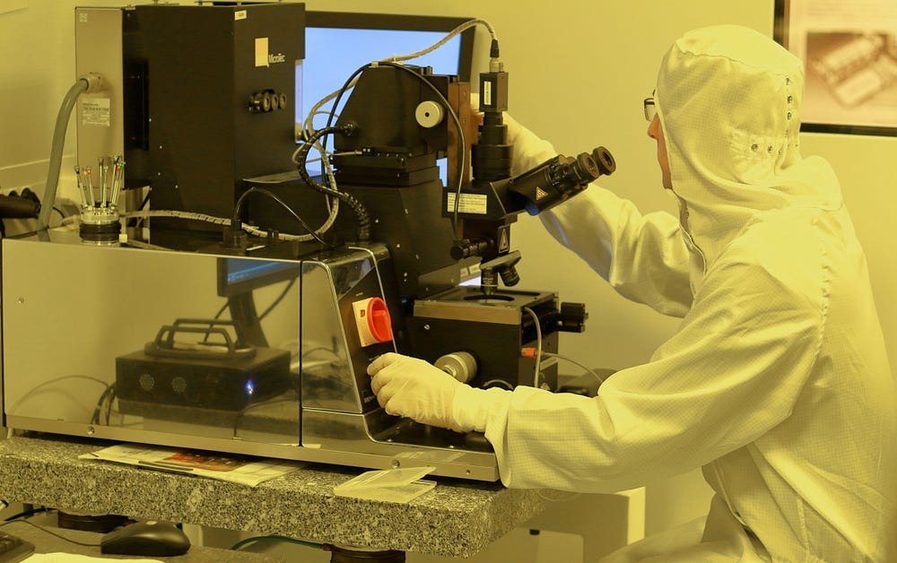
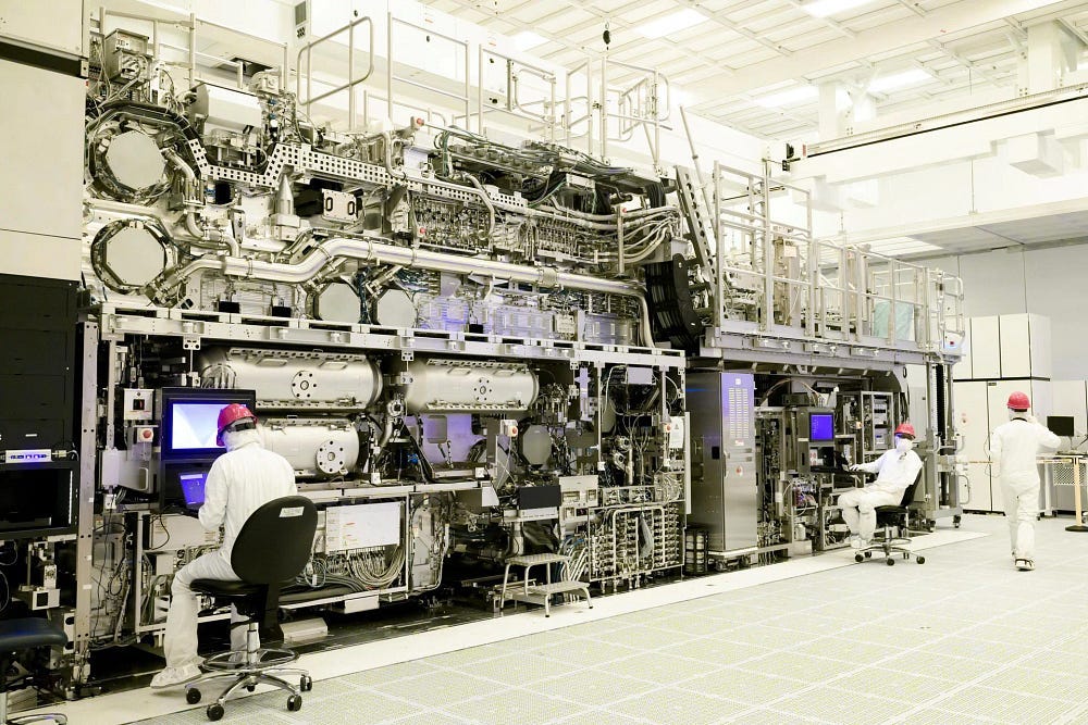
The most intricate device ever conceived by humankind is now in prototype form in China. Apart from the Netherlands, no other nation has the expertise to develop such a technology. Except this prototype fills an entire factory floor. For comparison, ASML’s EUV system, the machine that Europe and the United States refuse to sell to Beijing, is roughly the size of a school bus.
Same technology, objective, and wavelength. Except one fits in a room and the other needs a hangar.
If I’m leading with the size, it’s because understanding why it’s so big is the fastest way to understand exactly where China actually stands in this race. And more importantly, what it did differently from everyone else.
How You Print a Chip With Light That Doesn’t Exist in Nature
An EUV lithography machine is, at its core, a printer. But instead of depositing ink on paper, it prints microscopic circuits onto silicon.
The chips inside every computer, every car, every GPU running your AI workloads have all passed through a machine like this.
The more advanced the chip, the shorter the wavelength of light you need. The most advanced chips in the world require light at 13.5 nanometers, in the extreme ultraviolet range. You cannot buy this light. There is no EUV laser available anywhere. You have to manufacture it from nothing.
ASML’s method for doing this has always been spectacular, which is why it earned the machine its “science fiction” reputation. Every second, the system fires 50,000 microscopic droplets of tin into a vacuum. A first laser flattens each droplet into a tiny disc. A second, far more powerful CO₂ laser immediately strikes the same droplet. The tin transforms into a plasma at roughly 200,000°C, which, as it cools, emits light at exactly 13.5 nanometers. 50,000 moving targets per second, without missing a single one. ASML spent 20 years making this work reliably. Twenty years during which this approach became the absolute standard, the only known path to industrial EUV.
When China was cut off from this machine for geostrategic reasons, it faced a choice: either rebuild ASML’s method or find a different route to the same destination. Public reports suggest China is doing both in parallel, but the alternative approach is the one that surprised the industry.
The Method ASML Tested and Abandoned 20 Years Ago
It’s called Laser-assisted Discharge Plasma, or LDP. The principle is different. Instead of chasing 50,000 flying droplets, the LDP system uses two metal discs that rotate slowly through a bath of liquid tin. Each time the discs rotate, they coat themselves with tin. A laser vaporizes a small quantity of tin between the two discs. Then banks of capacitors discharge all their energy at once. The current passing through the vapor cloud generates a magnetic field that compresses the whole thing into plasma, and that plasma emits the same 13.5 nm light.
No giant CO₂ laser.
No need to aim at 50,000 targets per second.
Mechanically, it’s far simpler, maybe less spectacular, but potentially more efficient.
On paper, it sounds too good to be true. And it sounds too good because ASML tested exactly this approach 20 years ago and abandoned it. Not because it didn’t work, but because it didn’t produce enough light. Pumping more energy into the plasma just made it bigger, not brighter. The mirrors couldn’t capture enough useful photons. Output power plateaued at around 30 watts. A factory that’s trying to cook a meal with the heat from a light bulb.
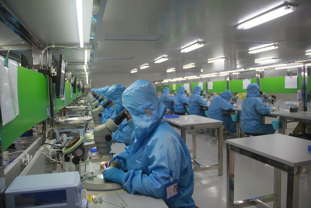
China made a bet. They bet that 2026 is not 2006. That 20 years of advances in materials science, simulation, and computational power would change the equation.
The early numbers suggest the bet is not absurd. Chinese prototypes are now achieving approximately 100 watts of EUV output, roughly three times what LDP produced when ASML abandoned it. But that’s still four to six times less than the 300–600 watts ASML’s production machines deliver today. And it’s far behind the 1,000-watt system ASML announced in early 2026. The gap remains massive. But twenty years ago, that gap didn’t exist at all, because nobody else had any EUV light source whatsoever.

The Mirrors That Only One Company on Earth Could Make
Producing the light, as difficult as that is, turns out to be only the first step. Once you have it, guide it to the silicon wafer where the circuit patterns will be printed. And at 13.5 nanometers, everything you know about conventional optics becomes useless. Glass doesn’t transmit this light. It absorbs it and swallows it whole. No lenses are possible. The only solution is extremely sophisticated mirrors: stacks of dozens of atomically thin layers of molybdenum and silicon, each surface polished to within 50 picometers. To grasp the absurdity of that precision: if one of those mirrors were scaled up to the size of Germany, the tallest bump would be one millimeter.
For 30 years, only one company on Earth knew how to make these mirrors: Zeiss, in Germany. This is not the outcome of one invention, but the product of thirty years of quiet refinement in polishing, coating, measurement, and alignment. Each Zeiss mirror reflects roughly 70% of EUV light. It might seem comfortable at first, but then you realize an EUV machine operates with 10 to 12 mirrors lined up. At each bounce, you lose 30%. What’s left of the original signal at the conclusion of the chain is quite minimal. And that’s with the best mirrors in the world.
The Changchun Institute of Optics (CIOMP) in China took on the challenge of recreating these mirrors without Germany. They partly succeeded. Their mirrors reflect approximately 65% of EUV light, five percentage points below Zeiss. Five points sound trivial, except that the loss compounds at every mirror. After 10 or 12 bounces, the Chinese system delivers less usable light than ASML’s meaningfully. When your light source already produces four to six times fewer watts at the start, you have a zero margin for error in the optics.
This is precisely why the Chinese prototype is so enormous. If your mirrors are less efficient and your light source is weaker, the only way to compensate is to make everything bigger: the collectors, the optical paths, and the mirrors themselves. If you can’t be more precise, you go larger. That’s why China’s machine fills a factory floor while ASML’s fits in something the size of a school bus.
The Strategic Calculation That Makes Size Irrelevant
While Beijing works on first-generation EUV, ASML is already shipping the next one. In July, Intel began producing its Core Ultra Series 3 processors using ASML’s High-NA EUV technology, which delivers nearly twice the resolution and enables chips below 2 nanometers. ASML plans to produce approximately 65 EUV systems this year, which is a 30% increase compared to last year. The target China is chasing doesn’t stand still. It accelerates.
Which raises the obvious question: what’s the point of a prototype that will already be a generation behind by the time it’s production-ready?
The answer lies in what’s happening in parallel. In late July, Shanghai Aishengna Electronic Technology Group began mass-producing domestic immersion DUV lithography machines.
Not EUV, but the previous generation. Boasting around $1 billion in capital, the company launched in August 2023 with support from two state shareholders.
No website.
No public communications.
Nobody in the industry had heard of them before this summer.
Five machines are planned for 2026 and 20 for 2027, with first deliveries going to SMIC, Hua Hong Semiconductor, and ChangXin Memory Technologies.
This matters because SMIC, China’s largest chip maker, currently uses a technique called quadruple patterning to fabricate its most advanced chips on existing DUV machines. The silicon wafer passes through the lithography machine four times for a single layer of detail. It works technically, but yields sit around 40%, meaning more than half the chips end up discarded.
Costs explode.
Production crawls.
And beyond 7 nanometers, the physics itself says stop.
Silicon Ruled Chips for 60 Years. Its Successor Is Three Atoms Thick.

Silicon has ruled the chip industry for 60 years. Every calculation happening on this planet right now, from your smartphone to the processors powering AI, runs on this one material. And for the first time, the industry has officially named what comes next.
China’s EUV machine doesn’t need to be the best in the world. It doesn’t even need to be commercially competitive against ASML. It just needs to be better than four DUV passes on the same wafer. If it can replace those four exposures with a single one, even with lower yields, even at slower throughput, that’s already a structural breakthrough for the Chinese chip industry. Not a global revolution, but a local one. And at Beijing’s scale, that’s more than enough.
China will need time to go from this prototype to a factory-ready tool running 24 hours a day, printing hundreds of wafers per hour for years without breaking down. But unlike ASML, this isn’t a commercial project. It’s a sovereignty project. The goal isn’t to sell machines to the world. It’s to build a machine that Beijing controls. That means the funding, the patience, and the political will be essentially unlimited by commercial standards.
The Twenty Years That Decided the Next Twenty
What’s playing out in this story goes well beyond lithography. What’s at stake controls the ability to manufacture the chips that will run artificial intelligence. Every large language model, every computer vision system, every autonomous agent that’s about to transform how you work in the next few years — all of it runs on chips that passed through a machine like this one.
The technological power balances of the next two decades are being decided right now, in cleanrooms, between mirrors polished to atomic precision and plasmas at 200,000 degrees. Most people do not know.
Understanding AI isn’t just knowing how to prompt a chatbot. Grasping the complexities of semiconductors, geopolitics, supply chains, and sovereignty is crucial for predicting who will control access to what in the future. That picture is more complete, more interesting, and more consequential than any single model benchmark.
If a factory-sized prototype might quietly reshape the chip war keeps you reading, follow us and subscribe; we cover the shifts that matter before they become consensus. For Science analysis, every piece, support us at the link below.